
Fabless semiconductor design · Pasadena, California
Denser signalling over copper
Our receiver decodes PAM6 and PAM8 links that conventional converters cannot resolve.
See the measurements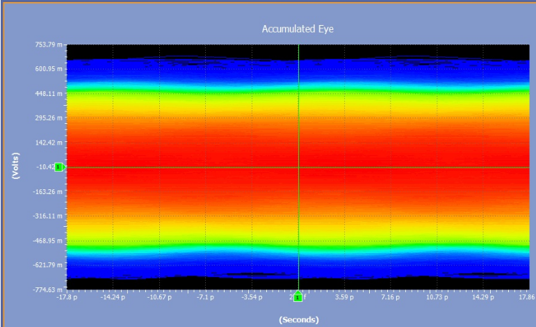
Traditionally, a lot of engineering goes into equalizing and filtering signals so the values don't blur together like they do in this readout. Even with a signal path as degraded as this, we get useful information.
The 400 Gb/s problem
Data center buildouts depend on moving from today's 100 and 200 Gb/s lanes to 400 Gb/s. The industry has always doubled lane rates by doubling the signal frequency. Doubling the signal frequency again would require signal bandwidth of 112 GHz, but copper attenuates sharply above 90 GHz. The standard approach gets much harder.
The alternative is to pack more bits into each symbol: PAM6 and PAM8 instead of PAM4. It needs no new chemistry, no new physics, and no precision manufacturing. But higher density modulation is really hard to get right.
Denser symbols sit closer together in amplitude, so signal integrity problems mean that errors overwhelm the greater data density. Because the different symbols are closer together in voltage, the same amount of noise has more of an effect at higher encodings. Additionally, timing error becomes more acute. Conventional analog-to-digital converters depend completely on a precise sampling clock. Running PAM6 at 400 Gb/s with a traditional converter would demand clock stability measured in single femtoseconds, which is very difficult to achieve.
What we do differently
We split analog-to-digital conversion into two stages.
Stage one: capture
A bank of simple filters
The incoming signal is decomposed into a set of frequency features. The components are crude, cheap, simple to manufacture.
Stage two: interpret
A lightweight neural network
Those features are mapped back to the digital value of the original signal. The network learns the behaviour of its own circuitry, not the content of the signal.
Because the filter bank captures redundant, overlapping information, the network can back-calculate physical distortions, including timing imperfections, rather than requiring the hardware to avoid them. The architecture makes no assumptions about the content of what is being transmitted.
Where we are now
Under an NSF SBIR Phase I award, we built and tested a physical prototype receiver and measured its performance. Under deliberately degraded timing it held a pre-FEC bit error ratio roughly forty times better than the 2.4×10⁻⁴ that IEEE 802.3dj standard requires with RS(544,514), and it worked cleanly with standard Reed–Solomon error correction.
We have since taken the architecture to 100G Ethernet line rates using commercial off-the-shelf components, and shown that the system can overcome the ISI, frequency attenuation, and thermal noise in an actual system at that speed.
What we're doing next
We want to run our system on faster and faster signals. We're simplifying our system, expanding our IP portfolio, and designing a dedicated chip for receiving signals at 400G.